The gradient of a line, also known as its slope, is a measure of its steepness. It describes the ratio of the vertical change to the horizontal change between any two points on the line. consider the diagram below:
Line A is closer to the vertical axis but farthest from the horizontal axis. Line A is said to be steepest among the lines A, B, C, D because it is the closest to the vertical line. The steepness of a line is it’s gradient.
consider yourself traversing through the lines horizontally via line Q and vertically via P.
You will arrive at A first while travelling horizontally but while moving vertically you will arrive at D first. D is closer to horizontal position but far from vertical position. The lines illustrated above are moving in two dimensions: Horizontal and vertical dimensions.
consider yourself moving along line B; you will realize that, you have changed horizontal and vertical distance in the movement.
As you move along B, you will have covered distance PY vertically and distance QY horizontally. The ratio of vertical distance covered to the horizontal distance covered gives the gradient(steepness of a line).
$$gradient = \frac{PY}{QY}$$
If vertical distance covered is larger than the horizontal distance, the line is said to have a steep gradient.
We can get gradient of a line by finding vertical and horizontal change from any two arbitrary points on a line.
Let us take any two points on a Cartesian plane shown above, x1 corresponds to y1 and x2 corresponds to y2.
the horizontal distance covered between P and Q = x1 -x2
the vertical distance covered between P and Q = y1 – y2
Electronics Exam Questions tests the broad areas of the field. Among the concepts tested by most of examiners includes, including basic concepts, analog circuits, and digital electronics. The subtopics to consider includes:
Ohm’s Law and basic circuits
Capacitors and inductors
Diodes and rectifiers
Transistors (BJT and FET)
Operational amplifiers (Op-Amps)
Logic gates and combinational circuits
Sequential logic circuits and number systems
Power supplies and regulation
circuit combinations
Below are some questions that are asked in examinations
(a) Distinguish between semiconductor and conductors (2mks)
(d) Figure 8 shows a puzzle box containing two lamps and other simple components connected so that, when terminal T1 is connected to the positive pole of a cell, Lamp L1 alone lights but when terminal T2 is connected to the positive lamp L2 alone lights.
Sketch a possible arrangement including lamps L1 and L2 and a set of diodes. (2mks)
2. (a) i) Explain how the resistance of semi-conductors and metal conductors are affected by temperature rise. (2mks) ……………………………………………………………………………………………………………………………………………………………………………………………………………………………………………………………………………………………………………………………………………………………………………………………………………………………………………………………………………………………………………………………………………………………
(b) ii) Sketch a forward bias characteristic of a P – N junction diode in the axis below.(1 mark)
3. a) A transformer is connected to a d.c source. The secondary coil is connected to a centre zero galvanometer.
State and explain the observation made on the galvanometer. (2 mks)
b) State Lenz’s law. (1 mark)
(i) Distinguish between semi conductors and conductors. (2 mks)
(ii) Give one example of a semi conductor and one example for a conductor. (2 mks)
(iii) What is meant by donor impurity in a semi conductor. (1 mk)
(iv) Draw a circuit diagram including a cell, a diode and a resistor in the reverse biased mode. (1 mk)
(v) In the circuit in figure 12 below, when the switch is closed, the voltmeter shows a reading. When the cell terminals are reversed and the switch is closed the voltmeter reading is zero.
The Intrinsic semiconductors are extremely pure semiconductor. A good example of such elements includes silicon(Si), germanium(Ge),Selenium(Se) and Tellurium (𝑇𝑒). These semiconductors have their outmost shell occupied by 4 electrons .
Their outer most electrons combines covalently with electrons from their neighboring atoms to form a crystal. each atom is hence surrounded by 4 other atoms.
Silicon atoms bond covalently by sharing their four valence electrons with four other silicon atoms, forming a stable, three-dimensional tetrahedral network. Each silicon atom is bonded to four neighbors, and each bond consists of a shared pair of electrons, which helps the silicon atoms achieve a stable outer shell configuration. The figure below illustrates formation of silicon structure.
At absolute zero temperature(-273.16K), the semiconductor crystal is an insulator. At room temperature, some electrons in the valence band gains enough energy to move to the conduction band leaving behind holes in the valence band. This movement makes the element a conductor. At higher temperatures, more electron are moved to the conduction bands and more holes are created. This increases the conductivity of the semiconductor material.
In an intrinsic semiconductor, the number of electrons equals the number of holes.
charge carriers
The electrons and the holes are referred to as the charge carriers. Small quantities of impurities may be added to an intrinsic semiconductors to enhance it’s conductivity on a process known as doping. An intrinsic semiconductor to which impurities have been added to enhance conductivity is referred to as an extrinsic semiconductor. Extrinsic semiconductors can be classified as either n-type or p-type semi-conductor. Depending on the type of semi-conductor created from doping, we develops majority and minority charge carriers.
Majority and minority charge carriers are electrons and holes that carry electric current in a semiconductor. Majority charge carriers are the most abundant type while minority charge carriers are the lesser in number.
The n-type semiconductors
This is formed by doping an intrinsic semiconductor with a pentavalent atoms. A pentavalent atom is an atom that has five valence electrons in its outermost shell. These elements belong to Group 15 of the periodic table, also known as the pnictogens. Pentavalent atoms are primarily found in the nitrogen group (Group 15) of the periodic table and include: Bismuth (Bi),Nitrogen (N),Phosphorus (P),Arsenic (As)and Antimony (Sb).
When a pentavalent atoms is introduced into the impure semiconductor,4 of it’s 5 electrons forms a covalent bond with 4 neighboring atoms of the intrinsic semiconductor.
This causes to be a free electron that is not bound to an atom. This free electron can thus be used for electrical conductivity.
Note: n-type semiconductor is electrically neutral since the total number of electrons is equal to the total number of protons in the material.
The atom added to the intrinsic semiconductor is referred to as the donor atom. For pentavalent atoms, they can also be referred to as the n-type impurity.
The P-type semiconductor
This is a type of semiconductor obtained by doping an intrinsic semiconductors with trivalent atoms.
Trivalent atoms are atoms that have a valence of three, meaning they have three electrons in their outermost shell or can form three covalent bonds. Examples include boron (B), aluminum (Al), and nitrogen (N) and Indium.
As an example, consider a boron atom being injected into silicon atom. Because boron has three electrons in it’s outer shell, it will have one electron less to complete the bonding when fitting into the silicon lattice. There will thus be a vacant place due to the missing electron which is a hole. The silicon crystal thus becomes an extrinsic semiconductor with holes as the majority charge carriers. The resulting semiconductor is referred to as the P-type semiconductor because the majority charge carriers are holes with an effective positive charge.
Illustrating hole as the majority charge carrier in a p-type semiconductor
Germanium doped with boron to form p-type semiconductor
A trivalent atom that completes bonding in an intrinsic semiconductor with one atom less to create a hole is known as an acceptor atom.
Electrons are minority charge carriers while holes are the majority charge carriers in a p-type extrinsic semiconductor.
The p-type semiconductor however, is not positively charged but electrically neutral. This is because the impurity introduces equal number of electrons and protons found in the nucleus.
Fixed ions
In P-type semiconductor holes are the majority charge carriers. As holes moves away from the parent atom, they make the atom to be a negative ion which is fixed in the crystal. This ion does not take part in conduction. electrons which are thermally generated exists as the minority charge carriers. See the illustration below.
In the n-type semiconductor, an electron moving away from a parent atom generates a fixed positive ion. The holes are thermally generated while electrons are as a result of doping. The figure below shows the fixed ion from the n-type semiconductor.
Electronics is the branch of physics and engineering that deals with the behavior and control of electrons to process information or control systems. The technology is based on circuits made of components that manipulate electrical signals, and it is the foundation of almost all modern devices, from consumer gadgets to industrial machinery.
Development of electronics has resulted to manufacture of appliances such as television sets, computer motherboards, radio-receivers, hi-fi systems, smart watches, etc. modern electronics devices are based on understanding properties of conducting materials.
Understanding of electricity and conductivity of various materials has enabled us develop electronic components such as diodes and transistors. These are very useful in controlling of electric currents.
Materials used to construct electronic components maybe classified as conductors, insulators and semi conductors. The differences in electrical properties among these materials depends on the force that holds the outermost electrons to the atoms of the material.
Conductors
This are materials with low electrical resistance. They carries electrical charges in them from one point to another. Their conductivity is facilitated by their internal structure.
The outermost electrons of the atoms in a conductor are loosely held such that they becomes detached to move freely through the material. The movement of these electrons facilitates conduction of current.
Resistance of current in metal is as a result of collisions between the freely moving electrons and the vibration of atoms. Increase of temperature increases the speed of vibrating atoms. The increase vibration increases the frequency of vibration. This increases the resistance of conductors hence resistance in metal increases with increase in their temperature. examples of conductors includes iron, copper, aluminium, lead, brass etc.
Insulators
They are materials with very high electrical resistance. Their outmost electrons are held tightly to their atoms and so they do not have free electrons. Insulators do not conduct electric current nor heat as they do not have free electrons to do so. However, insulators are very useful as they help in handling of materials that are carrying current or at high temperatures. Examples of insulators includes rubber, plastics , ceramics and wood.
semiconductors
They are the most useful as far as the electronics is concerned. These are materials with conductivity that is between that of conductors and that of insulators. Semiconductors allows the flow of electric current or heat under certain circumstances only. pure semiconductors have four electrons in their atoms outermost shell. They electrons are tightly held to the atom but the force that hold them is less compared to that in the insulators. However, the force is stronger than that of conductors.
At room temperature, the random atomic vibrations associated with the heat energy gives a small fraction of these electrons sufficient energy to escape from their bond and become free electrons. This causes them to be able to conduct electric current.
The escape of electrons from the structural bond leaves a gap where it was occupying.
The gap left by the escaped electron is known as the hole. Holes can hop from one atom to the other and responds to electrical voltage just like the electrons. However, holes carries positive charge while electrons carries negative charge. The figure below illustrates the movement of a hole during electrical conductivity of a semi-conductor.
Holes are the bonds between atoms where an electron has left the atom. Holes hop from atom to atom as shown:
As the temperature of a semiconductor is raised, the bond that holds electrons is weakened. More electrons are able to escape and so the number of free electrons and holes increases. This means that the electrical resistance of semiconductor decreases with increase of temperature. The reverse in conductivity is also true when temperature reduces.
The conduction band theory
In an atom, each electron has a specified amount of energy it posses. Each electron is thus said to exist in a certain energy level.
According to the energy-band theory, when two or more atoms are brought close to each other, the energy levels split into smaller energy levels called bands. This results from interaction of both electric and magnetic fields of the electrons as they revolve in their energy levels. The energy bands are illustrated below:
In solids, because atoms are close together, energy levels merge into bands of energy. Between the bands are gaps that represents energies electrons cannot have. It is the width of the gap that determines conductivity of the material.
The bands have gaps between them which represents energies electrons cannot have.
conduction band
The conduction band is the lowest energy band in a solid where electrons can move freely and conduct electricity. It is located above valence band and is typically empty or partially filled. When electrons gain enough energy, they can jump from the valence band to the conduction band.
Electrons in the conduction band can move freely through the material under the influence of an electric current.
The outermost electrons of the atoms occupies the conduction band and are not bounded exclusively to any one atom. The slightest potential difference across a metal will make the electrons flow. This makes metal good conductors of electric current and where current flow is proportional to the potential difference across the metal. Conductors have no energy gaps such that conduction band and the valence band overlaps. see the figure below:
valence band
The valence band is the highest energy band in a solid that is filled with electrons at absolute zero temperature. These electrons, called valence electrons, are the outermost electrons of the atoms and are responsible for chemical bonding. In valence band, electrons are not free to move.
Energy bands in semi-conductors
In semiconductors, there exists an energy gap between the valence band and the conduction band. An electron in a covalent bond between two atoms must receive extra energy in order to be lifted into the conduction band.
A significant number of electrons receives enough energy from thermal vibrations to be excited into the conduction band. This is because the gap allows.
When temperature rises, it increases the chance of electrons moving from valence band to the conduction band. Therefore electrical resistance of a semiconductor reduces with increase of temperature.
Energy bands in insulators
Insulators are as important in electronics as the conductors and semiconductors. The gap below the conduction band is very large and normal thermal vibrations are not sufficient to excite electrons into the conduction band. see the figure below.
There will never be any electron in the conduction band as the electrons remains bonded to their individual atoms hence cannot move as current. Temperature will not increase conductivity as there can never be found enough energy to excite an electron into the conduction band.
The decay law is an exponential decay law that describes the spontaneous transformation of unstable atomic nuclei into more stable ones by emitting radiation.
The decay law states that the rate of disintegration at a give time is directly proportional to the number of nuclides present at that time.
Radioactive decay is described as a spontaneous, random process in which the nuclide that will disintegrate next cannot be predicted. Time and chances determines the next nuclide to decay.
let N be the number of nuclides present at the current time.
then rate of change of N (dN) in respect to change of time(dt) is directly proportional to the existing number of nuclides available. That is:
$$\frac{dN}{dt} ∝ -N$$
Introducing a constant of the above proportionality which is known as the decay constant we get: λ
$$\frac{dN}{dt} = -λN$$
The negative sign in the equation above indicates that the number of nuclides N decreases with increase of time.
$$\frac{dN}{dt} \text{is referred to as the activity of the sample}$$
Half-life in radioactivity
Half life is the time taken for half of nuclides present in a radioactive sample to decay to half of their total number. For example if there 10000 nuclides in a sample, the time taken for them to reduce to 5000 due to radioactivity is the half life of the involved element.
It can be shown that the number of nuclides remaining undecayed , N, after a period of time T will be given by:
$$N = N_0 (\frac{1}{2})^{\frac{T}{t}}$$
The number of nuclides that remains after every half life can be plotted against a number of half lives to have the shape shown:
Example problems of decay law
The half life of a certain radioactive element is 16 years. What fraction of the element with have decayed after: (a) 48 years, (b) 80 years
solution
The amount remaining after T years will be given by:
from the above expression, it looks like we could easily get the summation of n numbers of items in an arithmetic series by simply adding two terms vertically. When arranged in reverse order, multiply by n then divide by two to get the sum.
From the above observations, we can easily add the the last term and the first term multiply by number of terms to get the sum x 2.
in other words; if there there are n terms in a series, if we have a term in m position, then am+a[n-(m-1)] = will always give the same value.
in the above series, let mth b the 7th term, then [n-(m-1)]th will be (10-7)th term = 3rd term.
consider the series s10 =5+9+13+17+21+25+29+33+37+41= 230
The 7th term = 29 while [n-(m-1)]th = [10-(7-1)]th term = [10-6]th term = 4th term.
The term in the series will be equal to 17.
29+17 = 46
To have a general expression, let us consider the general arithmetic series:
General expression of arithmetic series
sn = a+(a+d)+(a+2d)+(a+3d)+……..+[a+(n-3)d][a+(n-2)d]+[a+(n-1)d]
When radioactive materials undergoes radioactive decay, they produce radiations that exhibits different properties.
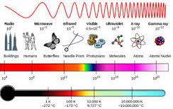
There are two broad categories of radiations: Ionizing radiation, which has enough energy to remove electrons from atoms and includes alpha particles, beta particles, neutrons, X-rays, and gamma rays. Non-ionizing radiation, which does not have enough energy to do so and includes radio waves, microwaves, infrared, and visible light. Ionizing radiation is further categorized into particle radiation (alpha, beta, neutrons) and electromagnetic radiation (X-rays, gamma rays).
One of the methods we use to distinguish among different radiations is how they behave inside magnetic and electric field. Figure below how a radiations from a radium source are deflected by magnetic field.
The radium source is placed in a thick lead box with a small opening. When a strong magnetic field is introduced perpendicular to the path of radiations, some are deflected . Using Fleming’s left-hand rule, we show that Radiation P is positively charged, R is negatively charged while Q carries no charge.
The positively charged radiation is called the alpha(α) radiations. The negatively charged radiations are referred to as beta (β) radiations.
The uncharged radiations are known as the gamma(γ) radiations.
From the diagram above, alpha particles are deflected the least suggesting that they are the heaviest. Alpha particles are basically helium nucleus
The energy of radiations is the energy carried by electromagnetic waves or particle radiation. It is directly proportional to the radiation’s frequency and inversely proportional to its wavelength. For electromagnetic radiation, this energy can be calculated using Planck’s equation, E = hf, where E is energy, h is Planck’s constant, and f is frequency.
The energy carried by a radiation determines the maximum kinetic energy gained by a photoelectron after it’s extracted to the metal surface.
A circuit shown can be used to investigate the relationship between the frequency of the radiation and the kinetic energy of the photoelectrons.
Frequency is varied using different color filters. for each color filter, the potential difference is varied by moving the jockey between X and Y until no current is registered. The battery is connected in such that it opposes the ejection of electrons by attracting the ejected photoelectrons back to the cathode. The voltmeter reading gives the stopping potential for a given frequency.
Different color filters will allow different frequencies to fall on cathode. This determines the energy of the photoelectrons and so the energy needed to stop them. Table below shows typical results obtained for stopping potential for radiations of varying frequencies.
Color
Frequency f(x 1014 Hz)
Stopping potential Vs
Violet
7.5
1.2
Blue
6.7
0.88
Green
6.0
0.60
Yellow
5.2
0.28
Orange
4.8
0.12
When a graph of stopping potential Vs against frequency f is obtained, it looks like the one shown below.
As can be observed, the graph is a straight line that cuts the horizontal axis at 4.5.
The equation of the graph can be fitted into the Einstein’s equation.
$$hf=hf_o +\frac{1}{2}mV^2 _{max}$$
The work done by the stopping potential is given by eVs
The work-energy theorem states that the net work done on an object is equal to the change in its kinetic energy. This means that when work is performed on an object, energy is transferred, causing its kinetic energy to increase or decrease.
From the work energy theorem;
$$eV_s = \frac{1}{2}mv^2 $$
substituting the above in the Einstein’s equation, we obtain:
$$hf= hf_o + eV_s$$
making the energy expression to be the subject we get;
$$eV_s = hf-hf_o $$
hence
$$V_s = \frac{hf}{e} – \frac{hf_o}{e}$$
however, hfo is the work function Wo of the metal.
From the graph, we can see that when Vs = 0;
$$\frac{hf}{e} = \frac{hf_o}{e}$$
and so f=fo
The graph of Vs against f therefore cuts the frequency axis at fo .
The slope of the graph is h/e and Vs intercept is -wo/e.
when we obtain the gradient of the graph, we can calculate the plank’s constant from the equation:
$$gradient = \frac{h}{e}$$
$$Y-intercept = \frac{-W_o}{e}$$
Values from energy of radiations graph
From our graphs above; we can obtain the threshold frequency of the metal using the equation:
$$eV_s = hf-hf_o $$
$$V_s = \frac{hf}{e} – \frac{hf_o}{e}$$
when Vs = 0;
$$\frac{hf}{e} = \frac{hf_o}{e}$$
and so f=fo
from the graph, the value of f at Vs=0 is 4.5 x 10¹⁴Hz which is the threshold frequency.
Energy of radiations from the graph
let us take two arbitrary points from the graph:(3,-0.51) and (8.4, 1.5)
Taxation is the process of collecting and managing tax collections. Tax are charges imposed onto individuals and profit making entities by government of the land. The government in return provides services to it’s citizens such as security, infrastructure, education etc.
Taxes can be direct or indirect.
Direct taxation
Direct tax includes taxes levied on incomes of individual persons and corporates.
Indirect taxation
Indirect tax is a tax imposed on goods and services before they reach the consumer who will pay tax on them. such tax is included in the market price of the goods or services and will be paid to the government by the seller of such goods and services. types of indirect services includes:
value added tax(V.A.T)- This are taxes levied on consumer goods and services
Exercise duty- for taxes levied on locally manufactured goods
custom duty- for tax levied on imported goods
Export duty- taxes levied on goods being exported
Income tax
Every one earning an income tax in a country is bound by law to give part of their income to the government as tax.
Amount of tax one should pay depends on the amount of income one receives.
sources of income could be salary, wages, commissions, interest on bonds, dividends from shares, profits from business activities etc.
The rate at which income tax is taken by the government are revised from time to time. New rates are made to take effect from 1st January of the following year.
Pay as you earn(PAYE)
PAYE is a system of tax collection whereby employers deduct tax from employee’s income to remit the tax to the government. The tax deducted is proportional to the income of the individual.For purposes of computing PAYE, an employer is required to apply the Individual Income Tax Rates (Bands) that range from 10% to 35% as per Finance Act and as tabulated by governing authority.
A typical to guide taxation based on income is shown
Monthly taxable income(Kshs)
Rate of tax
0-24,000
10%
24,001 – 32400
15%
32,401 – 59900
20%
59,901-120,000
25%
120,001 – 300,000
30%
above 300,000
35%
tax relief
2,400
The table above will be used to calculate tax due from salaried people in the country.
Tax relief
Tax relief refers to various deductions or exceptions that reduces the amount of tax to be paid from taxable income.
Taxation: Personal Relief
Personal Relief is granted to resident individuals.It is meant to lighten the tax burden on the taxpayer .
It is currently set at KShs 2,400 or KShs 28,800 per year .
Insurance Relief
Insurance relief is granted to an employee who has paid insurance premiums for life or health or education policies for himself, his wife or child.
Relief is given at 15% of premiums paid up to a maximum of Kshs 60,000 per annum.
For education and health, the policy has a maturity period of a t least 10 years.
Contains information related to marketing campaigns of the user. These are shared with Google AdWords / Google Ads when the Google Ads and Google Analytics accounts are linked together.
90 days
__utma
ID used to identify users and sessions
2 years after last activity
__utmt
Used to monitor number of Google Analytics server requests
10 minutes
__utmb
Used to distinguish new sessions and visits. This cookie is set when the GA.js javascript library is loaded and there is no existing __utmb cookie. The cookie is updated every time data is sent to the Google Analytics server.
30 minutes after last activity
__utmc
Used only with old Urchin versions of Google Analytics and not with GA.js. Was used to distinguish between new sessions and visits at the end of a session.
End of session (browser)
__utmz
Contains information about the traffic source or campaign that directed user to the website. The cookie is set when the GA.js javascript is loaded and updated when data is sent to the Google Anaytics server
6 months after last activity
__utmv
Contains custom information set by the web developer via the _setCustomVar method in Google Analytics. This cookie is updated every time new data is sent to the Google Analytics server.
2 years after last activity
__utmx
Used to determine whether a user is included in an A / B or Multivariate test.
18 months
_ga
ID used to identify users
2 years
_gali
Used by Google Analytics to determine which links on a page are being clicked
30 seconds
_ga_
ID used to identify users
2 years
_gid
ID used to identify users for 24 hours after last activity
24 hours
_gat
Used to monitor number of Google Analytics server requests when using Google Tag Manager